 |
|  |
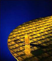
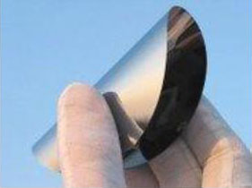
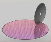
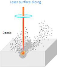
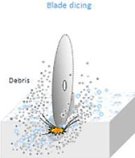
Wafer Dicing technologies
| Blade / saw dicing | 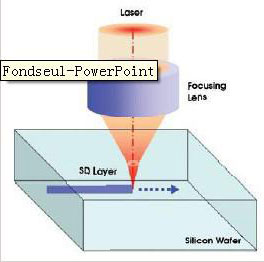 | Stealth dicing |
√Used for > 100um thick wafers ×Large Kerf (cutwidth) ×Chipping ×Debris/post clean ×Higher water consumption ×High consumable parts (blades) cost ×Not suitable for thin wafers | √Used for thin wafers < 100um √Dry process/ Enviro . Friendly √No debris ×IP protected process ×Not suitable for complex devices |
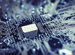
Wafer processing
 | 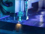 |  |
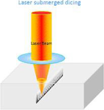
fs laser dicing laser ablation laser + saw | Full cut with Laser:only fs solution for thin wafers |
| √Hybrid technology offers high speed no mechanical forces;√no cracking or chipping √low kerf width √Low HAZ √High throug hput √Excellent yield, better accuracy √Hybridof laser + saw √Dry process, low material waste | √Low HAZ √No delamination √High through put √Excellent yield, high accuracy √Dry process, low material waste |
 |  |
|
Femtosec laser advantage
Multiple wavelengths available High power, high energy= high throughput High Reliability, good lifetime OEM solutions provider Manufacturing capacity Unmatched quality systems Global support structure, dedicated support available | Global support structure, dedicated support available Collaborative approach Industry leader in manufacturing of high power industrial laser systems Strong industrial links Strong partnerships with leading application laboratories |